PEOPLE
| Prof. Dimitrios Mataras | 2610969525 | dim@plasmatech.gr |
| Assoc. Prof. Eleftherios Amanatides | 2610969523 | lef@plasmatech.gr |
| Lecturer Nikolaos Spiliopoulos | 2610997451 | nspiliop@upatras.gr |
| Dr. Spyidon Sfikas | 2610969518 | spysfi@plasmatech.gr |
| Dr Ergina Farsari | 2610969518 | efarsari@plasmatech.gr |
| Dr Panagiotis Dimitrakellis | 2610969519 | pdimitrakellis@plasmatech.gr |
| Dr Ioannis Tsigaras | 2610969519 | tsigarasg@plasmatech.gr |
| Dr Villy Vrakatselli | 2610969521 | vvrakatselli@plasmatech.gr |
| Dr Ioannis Alexiou | 2610969521 | jalexiou@plasmatech.gr |
| Laboratory website: | http://www.plasmatech.gr | |
DESCRIPTION
PTLUP was founded in 1985 and since then it has been involved in research and education activities in the fields of Plasma Processing for the deposition of Thin-Films, Surface Treatment and Functionalization.
Plasma Processing is one of the most rapidly developing advanced technology fields dealing with the production and/or functionalization of new or enhanced materials for a wide range of high tech applications ranging from Microelectronics to Nanotechnology and MicroElectro Mechanics.
Our involvement in Plasma Processing covers both fundamental and technological aspects ranging from, plasma physics and chemistry to industrial plasma reactors design. Through the many research projects we have participated in, substantial expertise was gained specifically in the areas of plasma diagnostics and plasma modelling for the PE-CVD of various thin films among which thin film silicon for photovoltaic applications, either amorphous or microcrystalline (α–Si:H, μC-Si:H), holds a central position.
The methods initially developed for thin-film silicon were further exploited in a wide range of materials (SiOx, DLC, CFx, PDAA etc) and processes for a variety of applications (protective layers, wettability, biocompatibility, surface functionalization, plasma medicine etc).
EQUIPMENT
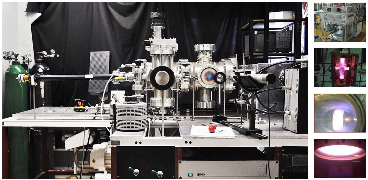
Plasma Technology Laboratory has designed and installed five different low pressure plasma reactors and three atmospheric pressure plasma systems for the deposition and surface treatment of different materials. The lab is also equipped with an advanced Scanning Probe Microscope suitable for thin films morphology measurements and calculations of electric, magnetic and thermal conductivity properties in the nanometer scale. In the same setup, a near – field optical microscope is adopted for improvement of nanoscale resolution and calculations of materials dielectric constant. Moreover, the lab possess an automated goniometer/surface energy analyzer with environmental chamber, while several setups of plasma diagnostics as electrical measurements, spectroscopic measurements, mass spectrometry and Laser Reflectance Interferometry are installed in the plasma reactors. Finally, for the simulation of plasma processes a cluster of PC’s is installed in the Lab suitable for modeling of large area industrial reactors.
More information and details for the Lab equipment can be found in the following link http://www.plasmatech.gr/index.php/facilities
PROJECTS - RESULTS
Plasma Technology Laboratory has participated and participates in a large number of European, National and Industrial projects. Information for these projects can be found in the following link http://www.plasmatech.gr/index.php/research/recearch-projects
The research and results of the lab are published in peer review international journals and in conference proceedings. All publication of the group can be found in the following link http://www.plasmatech.gr/index.php/publications